Part I:https://www.coursera.org/learn/build-a-computer (7 weeks, 6 projects, 1 computer and 0 prerequisite knowledge)
Part II:https://www.coursera.org/learn/nand2tetris2 (project-centered course)
Week 1 Boolean Logic
1.1 Boolean Logic
1.1.1 Boolean Identities
Commutative Laws
(x AND y) = (y AND x)
(x OR y) = (y OR x)
Associative Laws
(x AND (y AND z)) = ((x AND y) AND z)
(x OR (y OR z)) = ((x OR y) OR z)
Distributive Laws
(x AND (y OR z)) = (x AND y) OR (x AND z)
(x OR (y AND z)) = (x OR y) AND (x OR z)
De Morgan Laws
NOT(x AND y) = NOT(x) OR NOT(y)
NOT(x OR y) = NOT(x) AND NOT(y)
Idempotence Law
x AND x = x
Double Negation Law
NOT(NOT(x)) = x
1.2 Boolean Function
1.2.3 All Boolean Functions of 2 Variables
All Boolean Functions of 2 Variables
1.2.2 Truth Table to Boolean Expression
x
y
z
f
expression
0
0
0
1
NOT(x) AND NOT(y) AND NOT(z)
0
0
1
0
0
1
0
1
NOT(x) AND y AND NOT(z)
0
1
1
0
1
0
0
1
x AND NOT(y) AND NOT(z)
1
0
1
0
1
1
0
0
1
1
1
0
Write expressions that basically gets values of 1 only at the rows that have a value of 1, and OR them together:
(NOT(x) AND NOT(y) AND NOT(z)) OR (NOT(x) AND y AND NOT(z)) OR (x AND NOT(y) AND NOT(z))
= (NOT(x) AND NOT(z)) OR (x AND NOT(y) AND NOT(z))
= (NOT(x) AND NOT(z)) OR (NOT(y) AND NOT(z))
= NOT(z) AND (NOT(x) OR NOT(y))
1.2.3 Theorem
AND, OR and NOT
Any Boolean function can be represented using an expression containing AND, OR and NOT operations.
AND and NOT
Any Boolean function can be represented using an expression containing AND and NOT operations.
Proof: (x OR y) = NOT(NOT(x) AND NOT(y))
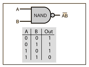
NAND
x
y
NAND
0
0
1
0
1
1
1
0
1
1
1
0
(x NAND y) = NOT(x AND y)
Any Boolean function can be represented using an expression containing NAND operations.
Proof:
NOT(x) = (x NAND x)
(x AND y) = NOT(x NAND y)
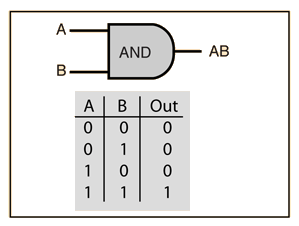
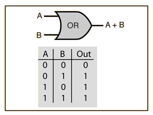
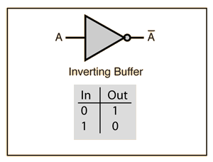
1.3 Logic Gates
1.3.1 Gate Logic
A technique for implementing Boolean functions using logic gates.
Logic gates:
Elementary (Nand, And, Or, Not, ...)
Composite (Mux, Adder, ...)
1.3.2 Elementary logic gates: NAND, AND, OR and NOT
NAND gateAND gateOR gateNOT gate
1.3.3 Composite Gates
(Three-way AND) gate interface:
three way AND gate
Gate implementation:
three-way and gate implementation
(One abstraction, many different implementations.)
1.3.4 CirCuit Implementations
circuit implementations with AND and OR gate
1.4 Hardware Description Language (HDL)
1.4.1 Design: from requirements to interface
Requirement:
Xor
General idea: out = 1 when (a AND NOT(b)) OR (b AND NOT(a)).
Implementation:
Xor implementation
1
2
3
4
5
6
7
8
9
10
11
12
/** Xor gate: out = (a AND Not(b)) Or (Not(a) And b)*/ Chip Xor{ IN a, b; OUTout;
PARTS: Not(in = a, out = nota); Not(in = b, out = notb); And(a = a, b = notb, out = aAndNotb); And(a = nota, b = b, out = notaAndb); Or(a = aAndNotb, b = notaAndb, out = out); }
Line 2 - 4: interface; line 5-11: implementation.
1.4.2 Some Comments on HDL
HDL is a functional / declarative language
The order of HDL statements is insignificant
Before using a chip part, you must know its interface. For example: Not(in =, out= ), And(a= , b= ,out= )...
Connections like partName(a = a, ...) and partName(…, out = out) are common
1.4.3 Hardware Description Languages
Common HDLs
VHDL
Verilog
...
Our HDL
Similar in spirit to other HDLs
Minimal and simple
Provides all you need for this course
HDL Documentation:
Textbook / Appendix A
HDL Survival Guide
1.5 Hardware Simulation
1.5.1 Simulation Process
Load the HDL file into the hardware simulator
Enter values (0's and 1's) into the chip's input pins (e.g. a and b)
Evaluate the chip's logic
Inspect the resulting values of:
The output pins (e.g. out)
The internal pins (e.g. nota, notb, aAndNotb, notaAndb)
1.5.2 Script-based Testing
An example of test script:
1
2
3
4
5
6
7
/** Xor.tst */

load Xor.hdl;
set a 0, set b 0, eval;
set a 0, set b 1, eval;
set a 1, set b 0, eval;
set a 1, set b 1, eval;
Benefits: "Automatic" and Replicable testing.
(Don't worry about how to write it. Because all the test scripts are available in the projects.)
1.6 Multi-Bit Buses
1.6.1 Examples
Addition of two 16-bit integers
1
2
3
4
5
6
7
8
9
10
/*
 * Adds two 16-bit values.
 */
CHIP Add16 {
  IN a[16], b[16];
  OUT out[16];

  PARTS:
  //...
}
1
2
3
4
5
6
7
8
9
10
11
/*
 * Adds three 16-bit values.
 */
CHIP Add3Way16 {
  IN first[16], second[16], third[16];
  OUT out[16];

  PARTS:
  Add16(a = first, b = second, out = temp);
  Add16(a = temp, b = third, out = out);
}
1
2
3
4
5
6
7
8
9
10
11
12
/*
 * ANDs together all 4 bits of the input.
 */
CHIP Add4Way {
  IN a[4];
  OUT out;

  PARTS:
  AND(a = a[0], b = a[1], out = t01);
  AND(a = t01, b = a[2], out = t012);
  AND(a = t012, b = a[3], out = out);
}
1
2
3
4
5
6
7
8
9
10
11
12
13
14
/*
 * Computes a bit-wise and of its two 4-bit
 * input buses
 */
CHIP Add4 {
  IN a[4], b[4];
  OUT out[4];

  PARTS:
  AND(a = a[0], b = b[0], out = out[0]);
  AND(a = a[1], b = b[1], out = out[1]);
  AND(a = a[2], b = b[2], out = out[2]);
  AND(a = a[3], b = b[3], out = out[3]);
}
1
2
3
4
5
6
7
8
9
/*
 * Buses can be composed from (and broken into) sub-buses.
 */
...
IN lsb[8], msb[8], ...
...
Add16(a[0..7] = lsb, a[8..15] = msb, b =..., out = ...)
Add16(..., out[0..3] = t1, out[4..15] = t2)
...
1.7 Project 1 Overview
God gave us a nand
1.7.1 Multiplexor
mux
A 2-way multiplexor enables selecting, and outputting, one out of two possible inputs
Widely used in:
Digital design
Communications networks
Example: using mux logic to build a programmable gate
AndMuxOrAndMuxOr implementation
1
2
3
4
5
6
7
8
9
CHIP AndMuxOr{
  IN a, b, sel;
  OUT out;

  PARTS:
  And(a = a, b = b, out = andOut);
  Or(a = a, b = b, out = orOut);
  Mux(a = andOut, b = orOut, sel = sel, out = out);
}
1.7.2 Demultiplexor
DMux
Acts like the "inverse" of a multiplexor
Distributes the single input value into one of two possible destinations
Example: Multiplexing/ demultiplexing in communications networks
Multiplexing/ demultiplexing in communications networks
Each sel bit is connected to an oscillator that produces a repetitive train of alternating 0 and 1 signals
Enables transmitting multiple messages on a single, shared communications line
A common use of multiplexing /demultiplexing logic unrelated to this course
1.7.3 And16
And16
A straightforward 16-bit extension of the elementary And gate
Whodunit story: Each suspect may or may not have an alibi (a), a motivation to commit the crime (m), and a relationship to the weapon found in the scene of the crime (w). The police decides to focus attention only on suspects for whom the proposition Not(a) And (m Or w) is true.
Truth table of the "suspect" function
1.8.2 Karnaugh Maps
The Karnaugh map (KM or K-map) is a method of simplifying Boolean algebra expressions.
Example:
A
B
C
D
0
0
0
0
0
0
1
0
0
0
1
0
2
0
0
1
0
0
3
0
0
1
1
0
4
0
1
0
0
0
5
0
1
0
1
0
6
0
1
1
0
1
7
0
1
1
1
0
8
1
0
0
0
1
9
1
0
0
1
1
10
1
0
1
0
1
11
1
0
1
1
1
12
1
1
0
0
1
13
1
1
0
1
1
14
1
1
1
0
1
15
1
1
1
1
0
Following are two different notations describing the same function in unsimplified Boolean algebra, using the Boolean variables A, B, C, D, and their inverses.
where are the minterms to map (i.e., rows that have output 1 in the truth table).
where are the maxterms to map (i.e., rows that have output 0 in the truth table).
imgIn three dimensions, one can bend a rectangle into a torus.
K-map drawn on a torus, and in a plane. The dot-marked cells are adjacent.
In the example above, the four input variables can be combined in 16 different ways, so the truth table has 16 rows, and the Karnaugh map has 16 positions. The Karnaugh map is therefore arranged in a 4 × 4 grid.
The row and column indices (shown across the top, and down the left side of the Karnaugh map) are ordered in Gray code rather than binary numerical order. Gray code ensures that only one variable changes between each pair of adjacent cells. Each cell of the completed Karnaugh map contains a binary digit representing the function's output for that combination of inputs.
After the Karnaugh map has been constructed, it is used to find one of the simplest possible forms — a canonical form — for the information in the truth table. Adjacent 1s in the Karnaugh map represent opportunities to simplify the expression. The minterms ('minimal terms') for the final expression are found by encircling groups of 1s in the map.
Minterm groups must be rectangular and must have an area that is a power of two (i.e., 1, 2, 4, 8…).
Minterm rectangles should be as large as possible without containing any 0s.
Groups may overlap in order to make each one larger.
The optimal groupings in the example below are marked by the green, red and blue lines, and the red and green groups overlap. The red group is a 2 × 2 square, the green group is a 4 × 1 rectangle, and the overlap area is indicated in brown. (The K-map for the inverse of f is shown as gray rectangles, which correspond to maxterms.)
Diagram showing two K-maps
Once the Karnaugh map has been constructed and the adjacent 1s linked by rectangular and square boxes, the algebraic minterms can be found by examining which variables stay the same within each box.
For the red grouping:
A is the same and is equal to 1 throughout the box, therefore it should be included in the algebraic representation of the red minterm.
B does not maintain the same state (it shifts from 1 to 0), and should therefore be excluded.
C does not change. It is always 0, so its complement, NOT-C, should be included. Thus, C' should be included.
D changes, so it is excluded.
Thus the first minterm in the Boolean sum-of-products expression is AC'.
For the green grouping, A and B maintain the same state, while C and D change. B is 0 and has to be negated before it can be included. The second term is therefore AB'. Note that it is acceptable that the green grouping overlaps with the red one.
In the same way, the blue grouping gives the term BCD'.
The solutions of each grouping are combined: the normal form of the circuit is.
Thus the Karnaugh map has guided a simplification of
It would also have been possible to derive this simplification by carefully applying the axioms of boolean algebra, but the time it takes to do that grows exponentially with the number of terms.
Don't Cares
Karnaugh maps also allow easy minimizations of functions whose truth tables include "don't care" conditions. A "don't care" condition is a combination of inputs for which the designer doesn't care what the output is. Therefore, "don't care" conditions can either be included in or excluded from any rectangular group, whichever makes it larger. They are usually indicated on the map with a dash or X.
The example above is the same as the example above but with the value of f(1,1,1,1) replaced by a "don't care". This allows the red term to expand all the way down and, thus, removes the green term completely.
This yields the new minimum equation:
f(A,B,C,D) = A + BC
Note that the first term is just A, not AC'. In this case, the don't care has dropped a term (the green rectangle); simplified another (the red one); and removed the race hazard (removing the yellow term as shown in the following section on race hazards).
First bit is -/+. All other bits represents a positive number.
Binary
Decimal
0000
0
0001
1
0010
2
0011
3
0100
4
0101
5
0110
6
0111
7
1000
-0
1001
-1
1010
-2
1011
-3
1100
-4
1101
-5
1110
-6
1111
-7
Complications:
Not obvious where to put the sign bit. To the right? To the left? (Early computers tried both.)
Adders may need an extra step to set the sign because we can’t know in advance what the proper sign will be.
-0?
2.3.2 1's Complement
The value is obtained by inverting all the bits in the binary representation of the number (swapping 0s for 1s and vice versa). The ones' complement of the number then behaves like the negative of the original number in some arithmetic operations. To within a constant (of −1), the ones' complement behaves like the negative of the original number with binary addition.
Offset binary, also referred to as excess-K, excess-N, excess code or biased representation, is a digital coding scheme where all-zero corresponds to the minimal negative value and all-one to the maximal positive value.
Example: Stardard excess of 4 bits: Excess-8 (2n-1)
Binary
Decimal
0000
-8
0001
-7
0010
-6
0011
-5
0100
-4
0101
-3
0110
-2
0111
-1
1000
0
1001
1
1010
2
1011
3
1100
4
1101
5
1110
6
1111
7
Complications:
Negate the signed number after operations
2.3.4 2's Complement (Preferred)
Represent negative number -x using the postive number 2^n - x.
Binary
Decimal
0000
0
0001
1
0010
2
0011
3
0100
4
0101
5
0110
6
0111
7
1000
-8 (8)
1001
-7 (9)
1010
-6 (10)
1011
-5 (11)
1100
-4 (12)
1101
-3 (13)
1110
-2 (14)
1111
-1 (15)
Positive numbers: 0, …, 2^(n-1) - 1
Negative numbers: -1, …, -2^(n-1)
Addition in 2's complement (for free):
Addition in 2's complement
Representation is modulo 2^n; addition is modulo 2^n.
2.3.5 Conclusion
Binary
Unsigned
Sign and Magnitude
1's Complement
2's Complement
Excess-8
0000
0
0
0
0
-8
0001
1
1
1
1
-7
0010
2
2
2
2
-6
0011
3
3
3
3
-5
0100
4
4
4
4
-4
0101
5
5
5
5
-3
0110
6
6
6
6
-2
0111
7
7
7
7
-1
1000
8
-0
-7
-8
0
1001
9
-1
-6
-7
1
1010
10
-2
-5
-6
2
1011
11
-3
-4
-5
3
1100
12
-4
-3
-4
4
1101
13
-5
-2
-3
5
1110
14
-6
-1
-2
6
1111
15
-7
-0
-1
7
2.3.6 Computing -x in 2's Complement
Input: x
Output: -x (in 2's complement)
Idea: 2^n - x = (2^n - 1) - x + 1
(2^n - 1 is 11...1 in binary.)
Example:
Input: 4
1111 - 100 + 1= 1100
Output: -4
To add 1: flip the bits from right to left, stopping the first time 0 is filpped to 1.
2.4 Arithmetic Logic Unit (ALU)
2.4.1 The Arithmetic Logic Unit
Computer System
The ALU computes a function on the two inputs and outputs the result.
ALU
f: one out of a family of pre-defined arithmetic and logical functions
Which operation should the ALU perform? That's a hardware / software tradeoff. Because if you choose not to implement something in hardware, you can always augment it later with sofeware.
2.4.2 The Hack ALU
The Hack ALU is a specific one that will hum inside our Hack computer.
Hack ALU
Operates on two 16-bit, 2's complement values
Outputs a 16-bit, 2's complement value
Which function to compute is set by six 1-bit inputs
Computes one out of a family of 18 functions
Also outputs two 1-bit values
zx
nx
zy
ny
f
no
out
1
0
1
0
1
0
0
1
1
1
1
1
1
1
1
1
1
0
1
0
-1
0
0
1
1
0
0
x
1
1
0
0
0
0
y
0
0
1
1
0
1
!x
1
1
0
0
0
1
!y
0
0
1
1
1
1
-x
1
1
0
0
1
1
-y
0
1
1
1
1
1
x+1
1
1
0
1
1
1
y+1
0
0
1
1
1
0
x-1
1
1
0
0
1
0
y-1
0
0
0
0
1
0
x+y
0
1
0
0
1
1
x-y
0
0
0
1
1
1
y-x
0
0
0
0
0
0
x&y
0
1
0
1
0
1
x|y
out
zr
ng
0
1
0
<0
0
1
>0
0
0
Pre-set the x input:
1
2
if zx then x = 0;
if nx then x = !x;
Pre-set the y input:
1
2
if zy then y =0;
if ny then y = !y;
Select between computing + or &:
1
2
3
if f
then out = x + y
else out = x & y
Post-set the output:
1
if no then out = !out
Result ALU output.
zr and zg:
1
2
if out == 0 then zr = 1 else zr = 0
if out < 0 then ng = 1 else ng = 0
2.5 Project 2 Overview
2.5.1 Half Adder
Implementation tip: it can be built using two very elementary gates.
sum: Xor; carry: And.
2.5.2 Full Adder
Implementation tip: it can be built from two half-adders with some other logic gates.
2.5.3 16-bit Adder
Implementation tips:
An n-bit adder can be built from n full-adder chips
The carry bit is "piped" from right to left
The MSB (most significant carry bit) is ignored
2.5.4 16-bit Incrementor
Implementation tip: the single-bit 0 and 1 values are represented in HDL as false and true.
2.5.5 ALU
Implementation tips:
Building blocks: Add16, and various chips built in Project 1
It can be built with less than 20 lines of HDL code.
Week 3 Memory
3.1 Sequential Logic
3.1.1 Combinatorial VS Sequential
Combinatorial:
out[t] = function(in[t]) (t= time)
operate on data only
provide calculation services (e.g. Nand … ALU)
Sequential:
out[t] = function(in[t-1])
operate on data and a clock signal
as such, can be made to be state-aware and provide storage and synchronization services
3.1.2 The Clock
Clock
3.1.3 Sequential Logic
state[t] = function(state[t-1])
Time & State
3.2 Flip Flops
3.2.1 Remembering State
Need an ingredient to remember one bit of infomation from time t-1 so it can be used at time t.
At the "end of time" t-1, such an ingredient can be at either of two states: "remembering 0" or "remenbering 1".
This ingredient remembers by "flipping" between these possible states.
Gates that can flip between two states are called Flip-Flops.
3.2.2 The "Clocked Data Flip Flop"
DFFDDF Timetable
Notational convention:
Notational convention
3.2.3 Implementation of the DDF
In this course: it is a primitive
In many physical implementations, it may be built from actual Nand gates:
Step 1: create a "loop" achieving an "un-clocked" flip-flop
Step 2: isolation across time steps using a "master-slave" setup
A cycle in the hardware connections is allowed only if it passes through a sequential gate
3.2.4 Sequential Logic Implementation
Sequential Logic Implementation
3.2.5 Remembering Forever: 1-bit Register
Goal: remember an input bit "forever" until requested to load a new value
1-bit Register
1
2
3
if load(t-1)
then out(t) = in(t-1)
else out(t) = out(t-1)
Working "Bit" Implementation
3.2.6 Multi-bit Register
Multi-bit Register
The width of a Register: w(word width): 16-bit, 32-bit, 64-bit, …
Register's state: the value which is currently stored inside the Register
3.3 Memory Units
3.3.1 Von Neumann Architecture
Computer System
3.3.2 Memory
Main memory: RAM (data + instruction), ...
Secondary memory: disks, ...
Volatile / non-volatile
3.3.3 The Most Basic Memory Element: Register
Register
To read the Register: probeout(which emits the Register's state)
To set Register = v: set in = v, load = 1 (and then from the next cycle onward, out emits v)
3.3.4 RAM Unit
RAM Unit
RAM abstraction: A sequence of n addressable registers, with addresses 0 to n-1.
At any given point of time, only one register in the RAM is selected.
Address: the location of the register within a larger chip.
k (width of address input): k = log_2(n) (For example, 8 register need 3 bits to represent.)
w (word width): No impact on the RAM logic (Hack computer: w = 16)
RAM is a sequential chip with a clocked behavior.
1
2
3
4
5
6
7
// Let M stand for the state of the selected register
if load then {
  M = in
  // from the next cycle onward:
  out = M
}
else out = M
3.3.5 RAM / Read Logic
To read Register i: set address = i (and then out emits the state of Register i)
3.3.6 RAM / Write Logic
To set Register i to v: set address = i, in = v, load = 1 (and then from the next cycle onward, out emits the state of Register v)
3.3.7 A family of 16-bit RAM chips
RAM8, RAM64, RAM512, ...
Chip Name
n
k
RAM8
8
3
RAM64
64
6
RAM512
512
9
RAM4K
4096
12
RAM16K
16384
14
3.4 Counters
3.4.1 Where Counters Come to Play
The computer must keep track of which instruction should be fetched and executed next
This control mechanism can be realized by a Program Counter
The PC contains the address of the instruction that will be fetched and executed next
Three possible control settings:
Reset: fetch the first instruction PC = 0
Next: fetch the next instruction PC++
Goto: fetch instruction nPC = n
Counter: a chip that realizes this abstraction.
3.4.2 Counter Abstraction
Counter Abstractio
1
2
3
4
5
6
7
if (reset[t] == 1)
then out[t+1] = 0 // resetting: counter = 0
elseif (load[t] == 1)
then out[t+1] = in[t] // setting: counter = value
elseif (inc[t] == 1)
then out[t+1] = out[t] + 1 // incrementing: counter++
else out[t+1] = out[t] // counter dose not change
3.5 Project 3 Overview
3.5.1 1-bit Register (Bit)
Implementation tip: it can be built from a DFF and a Mux.
3.5.2 16-bit Register (Register)
Implementation tip: it can be built from multiple 1-bit registers
3.5.3 8-Register RAM (RAM8)
Implementation tips:
Feed the in value to all the registers simultaneously
Use Mux / DMux chips to select the right register
3.5.4 RAM64, RAM512, …, RAM16K
Implementation tips:
A RAM device can be built by grouping smaller RAM-parts together
Think about the RAM's address input as consisting of two fields:
One field can be used to select a RAM-part
The other field can be used to select a register within that RAM-part
Use Mux / DMux logic to effect this addressing scheme
3.5.5 Program Counter (PC)
Implementation tip: it can be built from a register, an incrementor, and some logic gates.
3.6 End Notes
3.6.1 Nand to DDF
An SR latch constructed from cross-coupled NAND gates.
S'
R'
Action
0
0
Not allowed
0
1
Q = 1
1
0
Q = 0
1
1
No change
Week 4 Machine Language
4.1 Overview
4.1.1 Operations
operations
("100100" means addition...)
4.1.2 Program Counter
Program Counter
(We are now at instruction 159. Next instruction is 160...)
4.1.3 Addressing
Addressing
(Operate on memory location 340...)
4.1.4 Compliation
Program in nice high-level language (Python, Java, ...)
=Compiler==>
Program in machine language (based on CPU)
4.1.5 Mnemonics
Machine Language: 010001000110010
Assembly Language: ADD 1, Mem[129]
(location 129 in memory holds the "index")
ADD 1, index
A "Symbolic Assembler" can translate "index" -> Mem[129]
Interpretation 1: The "symbolic form" doesn't really exist but is just a convenient mnemonic to present machine language instruction to humans.
Interpretation 2: We will allow humans to write machine language instruction using this "assembly language" and will have an "Assembler" program convert it to the bit-form.
4.2 Elements
4.2.1 Machine Language
Specification of the Hardware/Software Interface
What are the supported oprerations?
What do they operate on?
How is the program controlled?
Usually in close correspondece to actual Hareware Architecture
Not necessarily so
Cost- Performance Tradeoff
Silicon Area
Time to Complete Instruction
4.2.2 Machine Operations
Usually correspond to what's implemented in Hardware
Arithmetic Operations: add, subtract, ...
Logical Operations: and, or, ...
Flow Control: "goto instuction X", "if C then goto instruction Y"
Differences between machine languages
Richness of the set of operations (divisions? bulk copy? ...)
Data types (width, floating point...)
4.2.3 Memory Hierarchy
Problem: Accessing a memory location is expensive
Need to supply a long address
Getting the memory contents into the CPU take time
Solution: Memory Hierarchy
4.2.4 Registers
CPUs ususlly contain a few, easily accessed "registers"
Their number and functions are a central part of the machine language
Data Register:
Add R1, R2
Address Register:
Store R1, @A
4.2.5 Addressing Modes
Register
Add R1, R2 // R2 ⬅ R2 + R1
Direct
Add R1, M[200] // Mem[200] ⬅ Mem[200] + R1
Indirect
Add R1, @A // Mem[A] ⬅ Mem[A] +R1
Immediate
Add 71, R1 // R1 ⬅ R1 + 73
4.2.6 Input / Output
One general method of interaction uses "memory mapping"
Memory location 12345 holds the direction of the last movement of the mouse
Memory location 45678 is not a real memory location but a way to tell the printer which paper to use
4.2.7 Machine Languages: Flow Control
Usually the CPU executes machine instructions in sequence
Sometimes we need to "jump" unconditionally to anothher location, e.g. so we can loop:
dest = null, M, D, MD, A, AM, AD, AND (M refers to RAM[A])
jump = null, JGT, JEQ, JGE, JLT, JNE, JLE, JMP (if (comp jump 0) jump to execute the instruction in ROM[A])
Semantics:
Compute the value of comp
Stores the result in dest
If the Boolean expression (comp jump 0) is true, jumps to execute the instruction stored in ROM[A]
Example:
1 2 3 4 5 6 7 8 9 10 11 12 13 14 15 16 17
// Set the D register to -1 D=-1
// Set RAM[300] to the value of the D register minus 1 @300 // A=300 M=D-1 // RAM[300]=D-1
// If (D-1 == 0) jump to execute the instruction stored in ROM[56] @56 // A=56 D-1;JEQ // if (D-1 == 0) goto 56
// Unconditional jump 0;JMP
// Set the A register to 1. Compute A-1 and store the value of the result in the M register, which is RAM[1]. Check if the computation is equal to 0. If true, the next instruction will be the value stored in the A register, which is 1. @1 M=A-1;JEQ
4.4 Hack Language Specification
4.4.1 The Hack Machine Language
Two ways to express the same esmantics:
Binary code
Symbolic language
The Hack Machine Language
4.4.2 The A-instruction: Symbolic and Binary Syntax
Symbolic syntax: @value
Example: @21
Binary syntax: 0value
Example: 0000000000010101 (Set the A register to 21)
4.4.3 The C-instruction: Symbolic and Binary Syntax
// Program: Flip.asm // flips the values of RAM[0] and RAM[1] // temp = R1 // R1 = R0 // R0 = temp
@R1 D=M @temp // using a variable M=D // temp = R1
@R0 D=M @R1 M=D // R1 = R0
@temp D=M @R0 M=D // R0 = temp
(END) @END 0;JMP
@temp: "find some available memory register (say register n), and use it to represent the variable temp. So, from now on , each occurrence of @temp in the program will be translated into @n"
Variables are allocated to the RAM from address 16 onward.
4.7.3 Iterative Processing
Example: compute 1 + 2 + … + n
Pseudo code:
1 2 3 4 5 6 7 8 9 10 11 12
// Computes RAM[1] = 1 + 2 + ... + RAM[0]

   n = R0
   i = 1
   sum = 0
LOOP:
   if i > n goto STOP
   sum = sum + i
   i = i +1
   goto LOOP
STOP:
   R1 = sum
// if i > n goto END @i D=M @n D=D-M @END D;JGT (END) @END 0;JMP
// RAM[arr+i] = -1 @arr D=M @i A=D+M M=-1
Week 5 Computer Architecture
5.1 Von Neumann Architecture
5.1.1 Von Neumann Machine
Stored program concept
Theory: Universal Turing Machine
Parctice: von Neumann Architecture
5.1.2 Elements
Elements
CPU
ALU: loads information from the Data bus and manipulates it using the Control bits
Registers: stores addresses and data
Memory
Data: put in an address of a data piece to be operated upon
Program: put in an address of the next program instruction
5.2 The Fetch-Execute Cycle
5.2.1 Fetching
Fetching
Put the location of the next instruction into the "address" of the program memory
Get the instruction code itself by reading the memory contents at that location
5.2.2 Executing
The instruction code specifies "what to do"
Execution involves accessing registers and/or data memory
5.2.3 Fetch-Execute Clash
Fetch-Execute Clash
Solution 1: Multiplex
Multiplex
Solution 2 (shortcut): Harvard Architecture - keep Program and Data in two separate memory modules
Computer System
5.3 The HACK Central Processing Unit (CPU)
5.3.1 The Hack CPU: Abstraction
The Hack CPU:
A 16-bit processor
Execute the current instruction
Figure out which instruction to execute next
5.3.2 Hack CPU Interface
Hack CPU Interface
Inputs
from Data Memory
inM: data value
from Instruction Memory
instruction: value of instruction
from the user
reset: reset bit
Outputs
to Data Memory
outM: data value
writeM: write to memory (yes/no)
addressM: memory address
to Instruction Memory
pc: address of next instruction
5.3.3 Hack CPU Implementation: Overview
Hack CPU Implementation
(c = control bits)
5.3.4 Hack CPU Implementation (1/3): Instruction Handling
Hack CPU Implementation ICPU handling of an A-instruction
CPU handling of an A-instruction:
Decode the instruction into:
op-code
15-bit value
Store the value in the A-register
Output the value (not shown in this diagram but in the overall)
CPU handling of an C-instruction
CPU handling of an C-instruction:
Decode the instruction into:
op-code
ALU control bits
Destination load bits
Jump bits
5.3.5 Hack CPU Implementation (2/3): ALU Operation
Hack CPU Implementation IIALU Operation: Input
ALU data inputs:
From the D-register
From the A-register
From the M-register
ALU control inputs (control bits):
From the instruction
ALU Operation: Output
ALU data outputs (result of ALU calculation):
To the D-register
To the A-register
To the M-register
(The feeding of the result is simultaneous, but which register actually depens on the instruction's destination bits.)
ALU control outputs
ALU control outputs:
Negative output?
Zero output?
5.3.5 Hack CPU Implementation (3/3): Control
Hack CPU Implementation IIIControl
Program Counter abstraction:
Emits the address of the next instruction
To start/restart the program's execution: PC = 0
No jump: PC++
(Unconditional) goto: PC = A
Conditional goto: if the condition is true, PC = A, otherwise PC++
5.4 The Hack Computer
5.4.1 The Hack Computer Abstraction
The Hack Computer Abstraction
Hack: a computer capable of running programs written in the Hack machine language, built from the Hack chip-set
5.4.2 The Hack CPU
Hack CPU Interface
The CPU executes the instruction according to the Hack language specifications:
If the instruction includes D and A (e.g. D=D-A), the respective values are read from, and/or written to, the CPU-resident D-register and A-register
If the instruction is @x (e.g. @17), then x is stored in the A-register; the value is emitted by addressM
If the instruction's right hand side includes M (e.g. M=M+1), this value is read from inM
If the instruction's left hand side includes M (e.g. M=M+1), the ALU output is emitted by outM, and writeM bit is asserted
If the reset==0, the CPU logic uses the instruction's jump bits and the ALU's output to decide if there should be a jump (and pc will emit the updated PC value)
If there is a jump: pc is set to the value of the A-register
If there is no jump: pc++
If the reset==1, pc=0 (causing a program restart)
5.4.3 The Hack Memory
The Hack Memory
Hack Memory abstraction:
Address 0 ~ 16383: data memory
RAM: 16-bit / 16K RAM chip
Address 16384 ~ 24575: screen memory map
Screen: 16-bit / 8K memory chip with a raster display side-effect
Address 24576: keyboard memory map
Keybord: 16-bit register with a keyboard side-effect
Decimal
Binary
0
0000 0000 0000 0000
RAM
...
...
RAM
16383
0011 1111 1111 1111
RAM
16384
0100 0000 0000 0000
Screen
...
...
Screen
24575
0101 1111 1111 1111
Screen
24576
0110 0000 0000 0000
Keyboard
5.4.4 Instruction Memory (ROM)
Instruction Memory
To run a program on the Hack computer:
Load the program into the ROM
Hardware implement: plug-and-play ROM chips
Hardware simulation: programs are stored in text files; program loading is emulated by the built-in ROM chip


where
are the minterms to map (i.e., rows that have output 1 in the truth table).
where
are the maxterms to map (i.e., rows that have output 0 in the truth table).


